What is a FPGA
What is FPGA
FPGA stands for Field Programmable Gate Array. It is an integrated circuit which can be “field” programmed to work as per the given design, hence it is termed as Field Programmable . It means it can work as a microprocessor, or as an encryption unit, or graphics card, or even all these three at once. At its core, an FPGA is an array of interconnected digital sub circuits that implement common functions while also offering very high levels of flexibility.
Beginners mostly use FPGA because of there cost effectiveness and reprogrammablility.
FPGA Design Flow:
One of the most important advantages of FPGA based design is that users can design it using CAD tools provided by design automation companies. Design flow of an FPGA includes following steps:
1) Design Entry: Design entry is done using two methods. One by schematic and second by HDL(Hardware Descriptive Language).
2)Synthesis: Synthesis is the process of converting input Verilog file into a netlist, which describes the connections between different block available on the desired FPGA chip.
3)Implementation: This phase where the layout of the design are determined. In the first step, the tool collects and analyzes the components like flip-flops, muxes and carry chains and organizes it in the cluster generated in packing stage. After the clustering process is done the tool starts the placement process and assign the components on there physical clustered position. In the next step all the parts are connected to each other. The tool tries to find every possible optimal path to connect all the parts.
4)Program: This is the final stage of the FPGA design where the FPGA is programmed according to the need of consumer. To do this the Bit stream file is generated and is dumped in the system using a flash programmer device.
FPGA Structural Classification:
Fundamental structure of a FPGA incorporates rationale components, programmable interconnects and memory. Course of action of these squares is explicit to specific producer. Based on inside course of action of squares FPGAs can be partitioned into three classes:
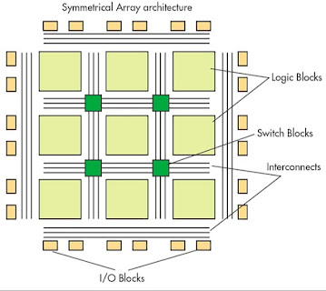
1) Symmetrical Array Architecture:
This architecture consists of logic elements (called CLBs) arranged in rows and columns of a matrix and interconnect laid out between them shown in Fig below. This symmetrical matrix is surrounded by I/O blocks which connect it to outside world. Each CLB consists of n-input Lookup table and a pair of programmable flip flops. I/O blocks also control functions such as tri-state control, output transition speed. Interconnects provide routing path. Direct interconnects between adjacent logic elements have smaller delay compared to general purpose interconnect.
2) Row based Architecture:
Row based architecture shown in Fig. below consists of alternating rows of logic modules and programmable interconnect tracks. Input output blocks is located in the periphery of the rows. One row may be connected to adjacent rows via vertical interconnect. Logic modules can be implemented in various combinations. Combinatorial modules contain only combinational elements which Sequential modules contain both combinational elements along with flip flops. This sequential module can implement complex combinatorial-sequential functions. Routing tracks are divided into smaller segments connected by anti-fuse elements between them.
Fig. Row Based Architecture
3) Hierarchical PLDs:
This architecture is designed in hierarchical manner with top level containing only logic blocks and interconnects. Each logic block contains number of logic modules. And each logic module has combinatorial as well as sequential functional elements. Each of these functional elements is controlled by the programmed memory. Communication between logic blocks is achieved by programmable interconnect arrays. Input output blocks surround this scheme of logic blocks and interconnects. This type of architecture is shown in Fig below.
Fig. Hierarchical PLDs
References : - [1] https://www.mepits.com/tutorial/169/vlsi/application-specific-integrated-circuit
[2] https://www.elprocus.com/application-specific-integrated-circuits/
[3] NPTEL
Author - Prasad Chatur


Very well explained
ReplyDeleteGood explanation
ReplyDeleteThanks
DeleteMuch helpful! 👍✌
ReplyDeleteThanks
DeleteWell written
ReplyDeleteThank you
DeleteWell done guys!!
ReplyDeleteThank you
DeleteNicely done !
ReplyDeleteVery nice work done
ReplyDeleteThanks
DeleteWell done
ReplyDeleteThanks
DeleteVery useful
ReplyDeletegreat work!
ReplyDeleteVery well written. Good content 👍
ReplyDeleteGood work guys. Keep it up👍
ReplyDeleteNice
ReplyDeleteThanks
DeleteGood Job.Nice work👍👍
ReplyDeleteThanks
DeleteGood explanation.Keep it up👍👍
ReplyDeleteThank you
DeleteGreat work.Informative👍
ReplyDeletegreat work guys 🙌🏻
ReplyDeleteVery nicely written 👍
ReplyDeleteThanks
DeleteNice work
ReplyDeleteVery useful ,nice explanation
ReplyDeleteThank you
DeleteGreat work
ReplyDeleteGreat work
ReplyDeleteGood👍
ReplyDeleteNice work
ReplyDeleteGreat Insight
ReplyDelete🙏
Deletenice write-up
ReplyDeleteThis comment has been removed by the author.
ReplyDeleteGood work. Keep it up!
ReplyDeleteGreat insight!!
ReplyDelete🙏
DeleteGood work
ReplyDeleteNice content
ReplyDeleteGood information
ReplyDelete🙏
ReplyDelete🙏
ReplyDeleteVery informative...
ReplyDeleteThank you
ReplyDeleteHighly informative 💯
ReplyDeleteContent well framed!! Good job👍!!
ReplyDeleteGood work
ReplyDeleteInformative👍
ReplyDeleteGood work
ReplyDeleteThis comment has been removed by the author.
DeleteThanks
Delete